
Building an IoT prototype is not just about selecting the right microcontroller, sensor, or wireless module. The PCB itself plays a major role in whether the prototype works reliably, fits the product size, survives testing, and can eventually move toward production.
In many early-stage projects, PCB decisions are made too quickly. Teams focus on features first, then treat the board as a simple carrier for components. That approach often creates problems later: unstable wireless performance, power noise, debugging difficulty, unnecessary board revisions, or a prototype that works in the lab but becomes difficult to manufacture.
Choosing the right PCB for an IoT prototype means thinking beyond basic connectivity. It requires balancing size, complexity, power needs, RF performance, assembly method, and future manufacturability.
Start With the Real Goal of the Prototype
Before choosing a PCB structure, it helps to define what kind of prototype you are actually building.
Not all IoT prototypes are the same. Some are proof-of-concept boards meant only to validate a function. Others are closer to engineering prototypes that need to test enclosure fit, wireless range, battery life, thermal behavior, or manufacturability. The more realistic the prototype needs to be, the more carefully the PCB should be planned.
For example, a quick functional demo board may tolerate a larger size, simpler layout, and hand assembly. A prototype intended for customer testing or pilot production usually needs better signal integrity, more stable power delivery, improved mechanical fit, and a PCB stack-up closer to the final product.
That is why the first question is not “How cheap can the board be?” but “What does this prototype need to prove?”
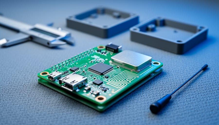
Choose the Right Board Size and Shape Early
In IoT products, board size is often more important than it first appears.
Many IoT devices are built around space constraints. Smart sensors, wearables, portable controllers, tracking devices, and connected home products usually have small enclosures and limited internal height. A PCB that is too large or awkwardly shaped can create problems with battery placement, antenna clearance, cable routing, or housing assembly.
At the prototype stage, it is tempting to leave extra board area “just in case.” A little margin is useful, but too much can hide layout problems that will appear later when the design is compressed. If the final product is expected to be compact, the prototype should move in that direction early enough to expose real design tradeoffs.
The PCB outline should also consider mounting holes, connectors, antenna keep-out zones, heat-sensitive areas, and assembly access. These details often matter just as much as component placement.
Think Carefully About Layer Count
One of the most important PCB choices is the number of layers.
A simple IoT prototype can often be built on a 2-layer board, especially if the circuit is low speed, physically large enough, and not heavily constrained by RF performance. For very basic sensor or control boards, that may be completely fine.
But once the design includes dense routing, compact placement, wireless modules, mixed analog and digital signals, USB, switching power supplies, or stricter EMC behavior, a 4-layer board often becomes the better choice.
A 4-layer board usually gives better ground continuity, cleaner power distribution, and more routing flexibility. It can also improve wireless and signal performance by providing more stable reference planes. That does not automatically make the board “high-end,” but it often makes the prototype behave more like a real product rather than a lab-only assembly.
In other words, reducing layer count may save money on the bare board, but it can increase design difficulty and create electrical compromises that cost more in debugging and redesign.
Pay Attention to Power Design
Many IoT prototypes fail not because the logic is wrong, but because the power design is weak.
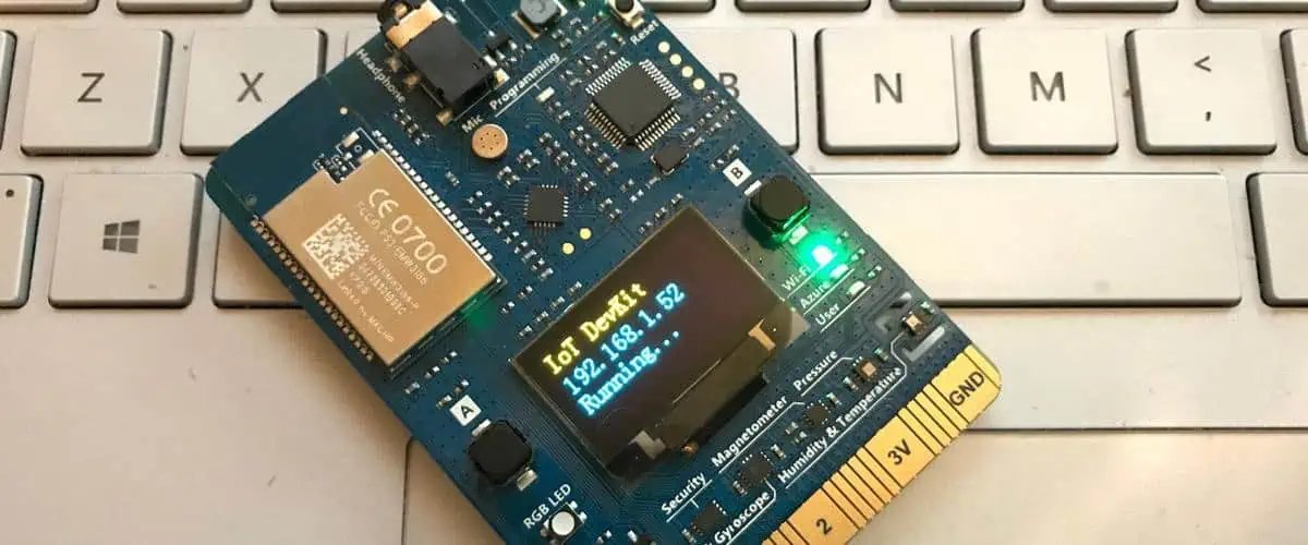
An IoT device may include a battery, USB input, charging circuit, sensors, a microcontroller, and a wireless transmitter all on the same board. Those blocks do not place the same demands on the PCB. If the layout is careless, noise from one section can affect another, voltage drop can become a problem, or peak current from wireless transmission can destabilize the system.
This is especially important in devices using Wi-Fi, LTE, NB-IoT, LoRa, or other wireless technologies that create burst current demands. A prototype may seem functional during light testing, then show resets, poor communication stability, or inconsistent battery behavior under real operating conditions.
When choosing the PCB approach, think about current paths, grounding strategy, decoupling placement, regulator layout, and whether the board needs better layer support for power integrity. These are not just layout details. They directly affect whether the prototype behaves like a usable device.
Wireless Performance Should Influence PCB Decisions
For many IoT products, RF performance is one of the most overlooked PCB-related issues.
If the design uses a wireless module or onboard antenna, the PCB is part of the RF system whether the team treats it that way or not. Board size, copper placement, nearby ground, shielding, connector location, and enclosure materials can all affect antenna efficiency and signal behavior.
Even when using certified modules, the PCB still matters. Poor antenna placement or a crowded layout can reduce range and stability enough to create false conclusions about the module itself. A weak PCB design can make a good wireless solution look unreliable.
That is why IoT prototype boards should reserve proper antenna clearance, follow reference layout guidance where available, and avoid turning the RF section into an afterthought. A prototype meant to evaluate connectivity must use a PCB layout that gives the radio a fair chance to perform.
Select Components With Assembly in Mind
At the prototype stage, engineers sometimes choose parts only by electrical function. That is understandable, but assembly should also be considered.
If the board is intended for quick hand soldering, very small packages may slow development and make debugging harder. If the goal is to test a design that may move into production later, using more realistic package choices can save time in the long run.
The right PCB for an IoT prototype is not only the one that can be routed. It is the one that can be assembled, tested, reworked, and revised without unnecessary pain.
This matters even more when compact boards begin using fine-pitch ICs, dense connectors, or RF sections with small passive components. A board that is technically manufacturable may still be inconvenient for iterative prototyping if every change becomes difficult to solder or inspect.
A good prototype board supports learning, not just first-pass functionality.
Design for Debugging, Not Just for Final Use
One common mistake in IoT prototyping is making the board too optimized too early.
A very compact, highly integrated PCB may look more product-like, but it can also make bring-up harder if test points, programming access, measurement points, or debug headers are missing. Prototype boards should still allow engineers to observe what the system is doing.
That means practical decisions such as:
- keeping access to key power rails
- leaving space for probing critical signals
- exposing reset, boot, or programming interfaces
- adding test points where troubleshooting is likely
- leaving limited flexibility for component value changes
A prototype board should not be messy, but it should be honest about the fact that debugging is part of the process.
Think About the Next Step: Prototype or Production Bridge?
A useful IoT prototype should reduce uncertainty, not create a dead-end design.
If the board is only meant for a one-time experiment, a simple and inexpensive layout may be enough. But if the project is likely to continue into pilot builds or small-batch production, it is worth making PCB choices that will scale more cleanly.
That includes realistic stack-up choices, manufacturable footprints, reasonable component spacing, and an assembly method that does not depend entirely on manual fixes. It also means avoiding layout shortcuts that make later redesign unavoidable.
The best prototype boards are not always the cheapest boards. They are the boards that help the project move forward with fewer surprises.
Common PCB Selection Mistakes in IoT Prototypes
Several mistakes show up again and again in IoT development:
Choosing 2 layers when the design really needs 4
This may reduce bare-board cost, but it often increases routing difficulty, weakens grounding, and makes RF and power behavior less stable.
Ignoring antenna layout requirements
Wireless performance problems are often blamed on firmware or module quality when the real issue is PCB layout or antenna clearance.
Making the board too large for convenience
A large board may be easier to route, but it can hide space conflicts that will become serious in later revisions.
Making the board too compact too early
The opposite problem also exists. Over-compressing the design can make debugging, rework, and early testing unnecessarily difficult.
Treating assembly as a later problem
Package size, spacing, and layout choices affect how quickly the board can be built and revised. Prototype-friendly design still matters.
Final Thoughts
Choosing the right PCB for an IoT prototype is really about deciding what the board needs to prove. A good prototype PCB should do more than connect components. It should help validate power stability, wireless behavior, mechanical fit, and overall design direction before the project moves further.
In many cases, the success of a prototype depends less on individual parts and more on whether the overall IoT PCB design is realistic, balanced, and easy to test. When board size, layer count, RF layout, power integrity, and debugging access are considered early, the prototype becomes far more useful as a step toward a reliable final product.